Digital Integrated Circuit (IC) design represents one of the most transformative and complex engineering disciplines of the modern era. It is the foundational technology behind every microprocessor, memory chip, and digital signal processor that powers our computers, smartphones, and countless other electronic devices. The journey from a high-level architectural concept to a physical, manufacturable chip on a silicon wafer is a meticulous and multi-stage process. This article outlines the key stages in digital IC design, tracing the path from VLSI system architecture down to the realities of CMOS fabrication.
1. The Starting Point: VLSI System Architecture
The design process begins not with transistors, but with ideas. The VLSI (Very Large-Scale Integration) system architecture phase involves defining the chip's overall function, performance targets, power budget, and area constraints. Architects create high-level block diagrams, specifying the major components like processors, memory controllers, input/output interfaces, and interconnects. They make critical decisions about the instruction set, pipeline depth, cache hierarchy, and parallelism (e.g., multi-core, SIMD). This stage is akin to drawing the blueprints for a skyscraper, determining its purpose, number of floors, and core structure before any detailed construction plans are made. Architectural exploration and modeling using high-level languages like C, C++, or SystemC are crucial to validate concepts and performance estimates before committing to hardware.
2. Register-Transfer Level (RTL) Design and Verification
Once the architecture is solidified, designers translate it into a hardware description language (HDL), primarily Verilog or VHDL. This stage is called RTL design. The code describes the circuit's behavior in terms of the flow of digital signals between hardware registers and the logical operations performed on them. It defines the exact functionality of each block—adders, multiplexers, finite state machines—in a cycle-accurate manner. Concurrently, functional verification is paramount. Engineers create extensive testbenches to simulate the RTL code, applying millions of test vectors to ensure it behaves correctly under all specified conditions. This phase catches logical bugs and ensures the design matches the architectural intent.
3. Logic Synthesis and Gate-Level Netlist
The RTL description, which is technology-independent, is then fed into a logic synthesis tool. This software maps the RTL code to a specific standard cell library provided by a semiconductor foundry (e.g., TSMC, Samsung). A standard cell library contains pre-designed logic gates (AND, OR, NOT, flip-flops) with characterized timing, power, and area data for a particular CMOS fabrication process (e.g., 5nm, 3nm). The output of synthesis is a gate-level netlist—a list of all the standard cells used and how they are interconnected. This netlist is a structural representation of the logic circuit. Timing analysis at this stage checks for setup and hold time violations to ensure the design will run at the target clock frequency.
4. Physical Design: From Netlist to Layout
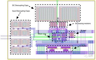
Physical design, or backend design, transforms the gate-level netlist into a geometric layout ready for manufacturing. This multi-step process includes:
- Floorplanning: Determining the overall shape of the chip, placing major blocks, and planning the power and clock distribution networks.
- Placement: Deciding the precise location of each standard cell on the silicon die.
- Clock Tree Synthesis (CTS): Building a balanced network to deliver the clock signal to all sequential elements with minimal skew.
- Routing: Creating the metal wires (interconnects) that connect the placed cells according to the netlist. Multiple layers of metal are used to manage complexity.
- Physical Verification: Running design rule checks (DRC) to ensure the layout adheres to the strict geometric rules of the fabrication process, and layout versus schematic (LVS) checks to confirm the layout matches the netlist.
5. The Foundation: CMOS Fabrication Technology
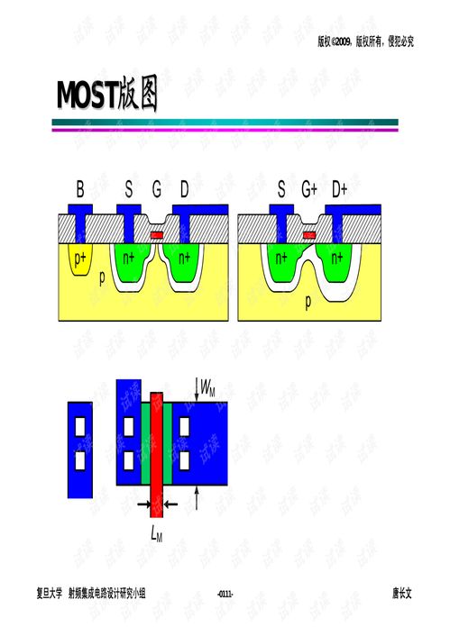
All modern digital ICs are built using CMOS (Complementary Metal-Oxide-Semiconductor) technology. The entire design process is constrained and enabled by the realities of the CMOS fabrication process, often called a process node (e.g., 7nm FinFET).
The fabrication process involves hundreds of intricate steps performed on silicon wafers in ultra-clean facilities (fabs). Key steps include:
- Photolithography: Using light and masks to pattern the wafer's surface.
- Etching and Deposition: Selectively removing or adding thin films of materials (silicon, silicon dioxide, metals).
- Ion Implantation: Doping silicon regions to create n-type and p-type transistors (NMOS and PMOS).
- Planarization and Metallization: Creating flat surfaces and building up the layers of metal interconnects.
The designer's standard cell library and design rules are abstractions of this immensely complex physical process. Factors like feature size (the smallest transistor dimension), interconnect parasitic capacitance and resistance, and power density (leakage current, dynamic power) are fundamental considerations that ripple up to influence architectural choices, RTL coding styles, and physical design strategies.
Conclusion
The design of a digital integrated circuit is a remarkable convergence of abstract thinking and physical science. It is a top-down journey that starts with architectural innovation and system-level modeling, progresses through rigorous logic design and verification, and culminates in a physical layout that must conform to the atomic-scale precision of CMOS fabrication. Each stage is deeply interdependent; a power-efficient architecture eases physical design, while fabrication limitations dictate the performance ceiling. Mastering digital IC design requires a holistic understanding of this entire pipeline—from the high-level VLSI architecture that defines what the chip does, down to the CMOS manufacturing process that determines how it is physically built. This end-to-end knowledge is what enables the creation of the ever-smaller, faster, and more energy-efficient chips that continue to drive the digital revolution.